Quantcast
Channel: Cadence Community
Viewing all 3331 articles
Browse latest View live

Plot issues in IC 615

$
0
0

 I have upgraded to IC 615 from IC 613. But I am facing problems:

1. In spectre RF when I do s parameter simulation and try to plot gain circles (Ga,Gp etc) I get nothing. Noise circles work well. I can plot the gain curves wrt frequency though which shows data is available.

 2. When I plot voltage conversion gain using pac then I get bar plot by default instead of solid line curve. Also in some plots I get in powers of ten form. How can I customize the plot?


How do I get the name of metal layers from the tech file

$
0
0

In the techParams section of my techfile, there are variables called "metal1_layer", "metal2_layer", ect, all set to the layer and pourpose pairs that show up in the LSW. 

Is there a way to get the layer name from the "metal2_layer" variable in the compiled techfile?  I would like to test to see if it is set, and if it is set obtain the name.

Pin rename

$
0
0

I have a script that places the pin in the appropiate place according to the lower pin place.

When I bring the pins in through VXL the pins are rectangle and the pin in the lower cell is a polygon. The script creates a polygon pin in the correct place, but I would like to keep the original pin name. I delete the original pin then try to rename to the old pin, but I get the error the original pin name already exists.

How do I purge the original name so I can rename the new pin name to the old?


Paul

Delete large number of shapes efficiently

$
0
0

I have a large number of shapes that I need to remove from the layout. I find that the delete command seems to take exponenentially increasing amounts of time to run as the number of shapes selected goes up. This creates the perverse situation where it is significantly faster to repeatedly select smaller groups and hit delete than to select them all at once and hit delete. Here's an example:

(note: delete here is the leHiDelete() )

 Select 29,000 objects all at once and hit delete -> ~81 seconds

Manually select a few thousand at a time and delete until all 29,000 are gone  -> 22 seconds


That's a huge difference since the 22 seconds includes all the time it takes for me to drag the mouse around in between delete commands. This gets worse the more objects are selected. Is there a more efficient way to do this? I tried writing a recursive delete function that breaks up large lists into smaller ones before deleting, but it doesn't seem to yield any speed improvement:

;; delete alias, speeds up deleting thousands of shapes
procedure( myDelete(@optional objects)
    if(objects == nil
        objects = geGetSelSet()
    );if

    cond(
    (objects == nil leHiDelete())
    (length(objects) < 1000 leHiDelete())
    (t
        info("splitting list of length %d\n" length(objects))
        b = copy(nthcdr(length(objects)/2 objects))
        rplacd(nthcdr(length(objects)/2-1 objects) nil)
        a = copy(objects)
        myDelete(a)
        myDelete(b)
    )
    );cond
)
 

custom menu

$
0
0

We are using Cadence 16.5 & I want to create custom menu for our CAD group.

First I added menu in allegro.men (...folder\share\pcb\text\cuimenus),

POPUP "&CAD Menu"
BEGIN
MENUITEM "&Bead Probe", "BeadProbe.il"
MENUITEM "set_refdes.il", "srd save"
END

I even added load("BeadProbe.il") and load("set_refdes.il") in allegro.ilinit

second, copy the Skill files to this location C:\Cadence\setup\pcbenv\skill

Now, when I open the database it loaded the CAD Menu, but when I select the command it show.

E- Command not found "srd save"

I tried both of the command and none of them is working.

Any advice would be greatly appreciated


Can't choose directory for netlist files

$
0
0

When netlisting from Design Entry CIS for the PCB editor, the dialog box is drawn with the right side of the box including the browse button for the Netlist Files Directory obscured.  It's a major painto have to type an absolute path into the box which not coincidentally doesn't show the whole path.   Resizing the window does not cure the issue, nor does changing tabs to try to force the window to redraw.  Another consequence is that the radio button label for Place Change Components Never is obscured in the same manner.

This is a new behavior since installing 16.6 on Win7 64 bit. 

 Is this a known problem?

The screenshot below shows the result after dragging the window wider.


A simple question about PCB antenna?

$
0
0

Have a question about PCB antenna in schematic. 

I am doing a design which include a bluetooth PCB antenna.This pcb antenna is only a trace. I am wondering should I put a schematic symbol of antenna in schematic, and then make a footprint of PCB antenna? Or leaving it along in schematic, and routing a trace of antenna in PCB layout? Which is the right way to do?


By the way, how to draw a trace in PCB layout, WITHOUT solder mask ? I want run a trace, with original color.

Thanks 

how cadence do to calculate Z11 in a psp analysis

$
0
0

hi,   

i'm simuliting a circuit, where i connect 4 switching caps to the port, than i run a psp annalysis to get the input impedance"Z11", and i want to know how spectre do to give such result, it's for helping me understandind how the input impedance behave.


PSPICE model

$
0
0

I'm using Virtuoso 6.1.5.

I downloaded a PSPICE model from a supplier.

However, it doesn't work because of syntax.


Could you give some advices to solve my problem?

(For the confidential reason, I have masked the specific number)


simulator lang=spice

.SUBCKT  model  20  10  30 Rg      10   1    1 M1      2    1    3    3    DMOS    L=XX   W=XX .MODEL DMOS NMOS (VTO={X.XX*{-X.XXX*TEMP+X.XXX}}  KP={XX.X*{X.XXXX*TEMP+X.XXXX}} + THETA=X.XXX  VMAX=X.XXX  LEVEL=3)  Cgs     1    3    XXXp Rd      20   4    XXm      TC=X.XXXX Dds     3    4    DDS .MODEL     DDS    D(BV={XXX*{X.XXXX*TEMP+X.XXX}}  M=X.X    CJO=XXXp    VJ=X.X) Dbody   3    20   DBODY .MODEL   DBODY    D(IS=X.X   N=X   RS=Xm   EG=X   TT=XX) Ra      4    2    XX       TC=XXX Rs      3    5    XXX     Ls      5    30   XXX M2      1    8    6    6   INTER E2      8    6    4    1    2 .MODEL   INTER    NMOS(VTO=X     KP=XX     LEVEL=1) Cgdmax  7    4   XXXX Rcgd    7    4    XXX Dgd     6    4    DGD Rdgd    4    6    XXXX .MODEL     DGD    D(M=XXX     CJO=XXXX     VJ=XXX) M3      7    9    1    1   INTER E3      9    1    4    1   -2

.ENDS model

simulator lang=spectre

Generate netlist with subckt statement for top level

$
0
0

I'm generating a netlist from CIW using:

simulator('spectre)
design("libName" "cellName" "viewName")
createNetlist()

This works fine but I would like to enclose the top level cell in .subckt/ends statements, similar to other cells in the hierarchy. Is that possible using the skill/ocean interface?


Thanks,

--Tavi

basics of thermal pad / power pad footprint creation

$
0
0

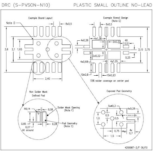
Hello, I'm new to Cadence, coming from Altium. I'm using Allegro Design Entry HDL and PCB Editor, rev 16.3.

As part of the new design and "new to designing with Cadence" process, I am creating parts for our library and I'm having some trouble with a TI SON part that includes a thermal pad or power pad. Here is a snap shot from the TPS6120:

 TI TPS61202 Footprint

At this point, I've made the pads in the padstack editor (but made them rectangles since I didn't know how to make it a rect at one end and rounded at the other) and used the symbol creation wizard to make a SOIC. To make the thermal pad I placed a filled polygon on the Etch/top layer and it is one large pad with the outline like above.

Question: How do turn my filled polygon into a ground pin (or should I not?) and how do I add the soldermask layer to something I've drawn like this?

Question: How do I add vias to my footprint? My plan was to create the via in the padstack editor then place them in the appropriate places but I have some confusion as to whether the pad/via structure is just supposed to sit there dangling or if it should be assigned a pin # (ground).

I did search the forum and came across the thread Thermal Pad Shape with Vias In it a poster mentions that he makes these pads using multiple surface mount style pins. I think I can figure out how to do this but I'd appreciate any tips on setting up the tools and pads so that things are properly done.

Picture of the pad made from pins:

pad of pins

Differential Pair routes with No Gap

$
0
0

Hi,

I'm using OrCAD PCB Designer and have created differential pairs. When I manually route the pair, the gap between traces is always zero no matter what I set the gap to in the contraints manager. I'm fairly new to this tool so I'm getting a littel frustrated why it does this. I even found another posting that some provided a .brd design with a diff pair and its own CM settings. When I deleted the traces to then reroute them, I found the same problem, the trace gap went to zero! Is this a license limitation or am I missing something? I've created CSet spacing parameters in the CM.

Thanks for any help that someone might be able to provide.

 -KC 

Pspice model errors in Virtuoso

$
0
0

 Hi Guys

I am trying to simulate MAX9643U and EL7202 (using their Pspice models) as a part of my design, in Virtuoso. While I have reviewed many similar problems and solutions in this informative website, I still can not overcome the errors.

1) MAX9643U
(the model is available here:
http://www.maximintegrated.com/design/tools/modeling-simulation/spice/current-sense-amps/orcad/MAX9643U.LIB)

The problem points to the line:

Fi+ RS+ GND VALUE={-I(Vi+)+20.02u}

I read in one of the posts that I have replace {} by ''. but the error still exists and says:
"Expected 1 controlling voltage sources, but found 0"

2) EL7202
(the model is available here:
http://www.intersil.com/content/dam/Intersil/documents/el72/el7202.txt)

The problem (I guess) is related to the lines below:

.model spmod vswitch ron=3 roff=2meg von=1 voff=1.5
.model snmod vswitch ron=4 roff=2meg von=3 voff=2
e1 out vss table {(v(inp)-v(inm))*5000} = (0,0) (3.2,3.2)

and  the error says:
"Error (CMI-2078): I1016.sn: Required parameter 'file' is missing"
"Error (CMI-2078): I1016.sp: Required parameter 'file' is missing"


Any comment is highly appreciated, in advance
Politekniko

Reqular expression in skill programmin

$
0
0

Can anyone explain me how to use use the regular expression in skill programming........

I'm geeting many info from cadence from that I want only PMOS and  NMOS information from this command geGetEditCellView()~>instances~>cellName

Result is  ("N_18_MM" "N_18_MM" "N_18_MM" "opin" "ipin" "ipin" "ipin" "ipin" "ipin" "ipin""ipin" "P_18_MM" "P_18_MM" "P_18_MM")

From this I want only  "N_18_MM" &"P_18_MM" info

opening a cell layout view in GUI mode using SKILL

$
0
0

Hi,

  How to open a layout view in GUI mode using skill code? I want to open a cell layout view in XL mode.

dbOpenCellViewByType will open the cell in background with specified library, cell name and mode, but how to open in GUI mode?? 


Regards,

Santhosh 


OrCad 16.6 Lite

$
0
0

Hi all,

I've just tried OrCad 16.6 lite version. I used capture cis to design a simple circuit, but I wasn't able to run Pspice because the assosiated toolbar was unabled.

Can anyone help to this?

Thanks in advance.

how create a ".cir" file in Orcad 16.3

$
0
0
Hello, 
I would like to create a "cir." file in Orcad 16.3 but I'm a little lost, is that you can help me? 
is and what you can tell me how to change the number of output bipolar transistors, ie, I find in the software transistors 3 terminals (EBC), while I want to add the substrate channel but I do not know how. and when I change the netlest and I run the simulation it removes all the changes I did. 
Thank you for your help.

Why can't I login to this forum with IE?

$
0
0

Just a repetitive problem I'm having.  My Win7 64-bit PC and IE10 will not let me log-in to the Cadence forum.  No errors, block notices or anything.  It just won't do it.  Log-in attempts spend a few secs "waiting circle" and then return me to the login screen.

Chrome on the other had has no problem from the same PC (i.e. I'm here now).

 Anyone got any Microsoft clues?

Regards, 

specctra quit unexpectedly with an exit code of 5

$
0
0

Hi guys, yesterday when I ran the command of 'automatic router ' in PCB Editor, the message ' specctra quit unexpectedly with an exit code of 5 ' was shown on the screen and I was confused , because I never seen it before.

 Then I looked the Specctra Log file and there are several error message shown below:


# <<WARNING:>> Potential non fixed positive shape alignment with the host CAD system exists.

#              Allegro PCB Router does not perform any operations to remove or identify slivers and isolations.

#              If the host CAD system performs such an operation, the user may experience unrouted

#              or DRC alignment issues.

#              The user must perform final unrouted/DRC validation within the host CAD system.

# <<ERROR:>> Error in file D:/BIT work/MB7K01/PCB\MB7K01.dsn, line 19668: token 5 = Orphan_net

# (content):   (wire (net Orphan_net) (type route))

# <<ERROR:>> Parser: Unrecognized token net while parsing shape 


I have no idea about  " line 19668: token 5 = Orphan_net "

Can anyone help me to solve it please?

 Thank you very much!

Block execution in SKILL file while a form is on the screen

$
0
0

Dear SKILL experts

I tried to write a SKILL function that shows a form created by hiCreateAppForm() on the screen and blocks execution until the form is removed from the screen by the user with a OK or Cancel.

In the form I have a listBoxField. The user selects ONE item in the listBox. When OK is pressed the SKILL function that showed the form returns the selected item, when Cancel was selected the function returns nil.

I tried the argument: ?dialogStyle 'modal but the form does not block the execution.

The code is in one SKILL file that I load but the execution of the SKILL statements in the file is not blocked while the form is on the screen.

Here is the code:

file listBox.il:


      ; Create the application form
      hiCreateAppForm(

        ?name 'VARselectListForm
        ?formTitle "Title"
        ?dialogStyle 'modal
        ?initialSize t
        ?buttonLayout 'OKCancel
        ?fields list(
          list(

            hiCreateListBoxField(
                ?name 'VARselectListFormListBox
                ?choices nil
                ?value nil
                ?prompt "Nodes"
            ) ; hiCreateListBoxField

            list(0 0)
            list(150 400)
            50
          ) ; list
        ) ; list

      ) ; hiCreateAppForm

 procedure(SHOWselectListBoxForm(title choices)

    when(and(boundp('VARselectListForm)
             hiIsForm(VARselectListForm))

        VARselectListForm->title = title
        VARselectListForm->VARselectListFormListBox->choices=choices

        hiDisplayForm(VARselectListForm)

        VARselectListForm->VARselectListFormListBox->value

    ) ; when

) ; SHOWselectListBoxForm

And the the file that uses this:

load("listBox.il")

choices = '("aaa" "bbb" "ccc" "ddd" "eee")
title   = "Form title"

printf("Before the box\n")
choice = SHOWselectListBoxForm(title choices)

printf("After the box: %L\n" choice) 

The message After the box............. already appears while the form is on the screen.
I want a blocking solution. The dialog style systemModal is gone.

 Of course I can make a wait loop with global variables, but is there a better way?

Hans Kok


Viewing all 3331 articles
Browse latest View live


<script src="https://jsc.adskeeper.com/r/s/rssing.com.1596347.js" async> </script>